
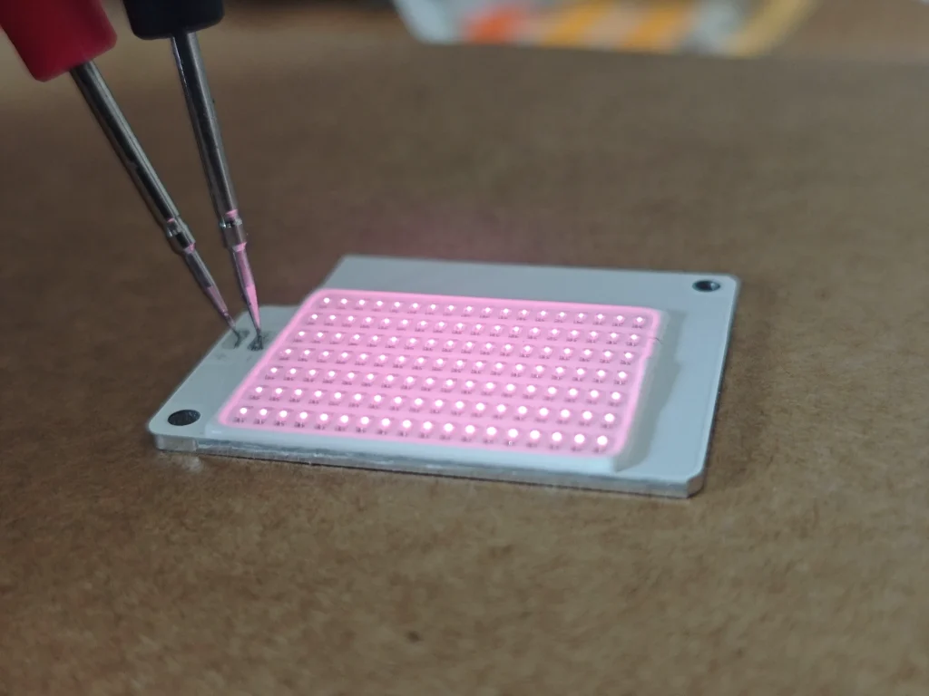
Infrared COB LED as a groundbreaking breakthrough, has completely revolutionized the chip packaging solutions in the field of infrared imaging. It integrates multiple chips directly onto the substrate through unique process design, which not only greatly improves the integration degree of the system, but also significantly enhances the clarity and detection range of the image, bringing a qualitative leap to infrared imaging technology.
How to customize COB LED products?>>
This innovative achievement has demonstrated outstanding effectiveness in many fields such as security monitoring, industrial testing, medical beauty, etc., and has become an important force in promoting industry development. In terms of security monitoring and night vision enhancement, high-power infrared COB LED light sources using COB packaging technology have played a huge role. These light sources cover multiple frequency bands such as 740nm, 850nm, and 940nm, and can be flexibly selected according to the needs of different application scenarios. They inject strong power into network cameras and car night vision systems, enabling devices to achieve high-definition infrared imaging effects even at long distances. In industrial production, precision detection and temperature monitoring are crucial links. The high-resolution infrared detection module implemented through COB packaging is gradually becoming a key component in industrial temperature measurement. This module has the advantage of being compact and lightweight, and can be easily integrated into various industrial devices, whether it is a complex production line or a small space, it can be perfectly adapted. Its application not only improves detection efficiency, but also greatly enhances measurement accuracy, providing strong support for production management and quality control of enterprises. Medical beauty, hygiene screening, and innovation in consumer electronics are also areas where COB technology has shown great potential. The cross-border application of infrared thermal imaging technology has extended to multiple aspects such as medical quarantine, and the introduction of COB packaging technology has further promoted the miniaturization process of related equipment, greatly expanding the market application space. Meanwhile, in the field of consumer electronics, COB technology also provides more possibilities for product innovation and upgrading, allowing ordinary consumers to enjoy the convenience brought by high-performance infrared imaging.
Go To See Our Various Custom COB LED Products Video>>
In terms of core advantages, COB technology directly optimizes the image quality performance of infrared imaging through wafer level precision packaging, innovative heat dissipation solutions, and efficient dust prevention mechanisms. Its unique packaging method ensures tight connections and stable operation between chips, reducing signal interference and energy loss. The innovative heat dissipation design effectively reduces the temperature during equipment operation and extends its service life. The efficient dust prevention mechanism ensures that the equipment can maintain good working condition even in harsh environments. With excellent photoelectric conversion efficiency and directional focusing design, COB technology has successfully broken through the detection distance limitations of traditional technologies, achieving a longer detection range and higher sensitivity. Combined with its simple structure and strong stability, COB technology has achieved the miniaturization transformation of equipment, promoting the widespread adoption of high-performance infrared imaging solutions and bringing good news to more industries and fields.